
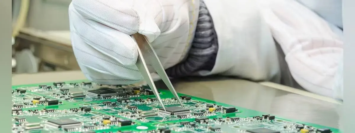
HDI PCB
High-density interconnect boards with fine lines, micro-vias and small holes for compact, high-performance designs.
Last updated
HDI PCB samples
-
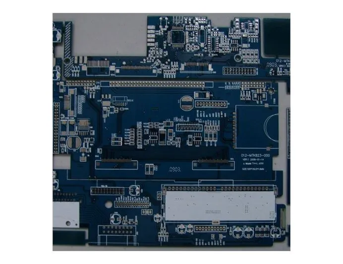
4L FR4 HDI board, thickness 1.6 mm, min. hole 0.25 mm
-
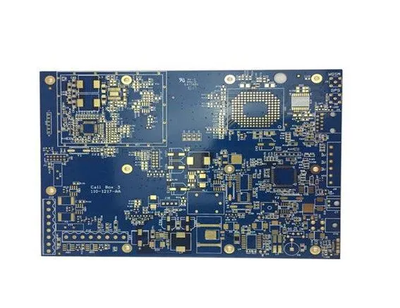
HDI board, immersion gold + OSP
-
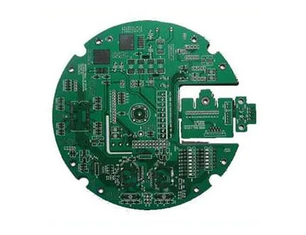
6L PTFE HDI high-frequency board, thickness 1.2 mm, immersion tin
About HDI PCB
High-density interconnect (HDI) boards fit more connections into less area by using finer lines and spaces, laser-drilled micro-vias, and blind and buried vias. That makes room to fan out fine-pitch BGAs and lets a design shrink in size or layer count without running out of routing space.
Our partner factories build HDI boards with laser-drilled holes down to 4 mil, track width and spacing down to 3 mil, and blind and buried vias, in FR4 as well as PTFE high-frequency materials. Finishes include immersion gold, OSP, a combination of both, and immersion tin.
Typical applications
- Smartphones and tablets
- Processor and memory boards with fine-pitch BGAs
- Compact industrial controllers
- Portable and medical instruments
- RF modules on PTFE material
Common questions
When do I need HDI instead of a standard multilayer board?
When the BGA pitch is too fine to fan out with through-hole vias, when the board has to get smaller, or when the routing would otherwise need many extra layers. HDI via structures free up space on the inner layers.
What is a micro-via?
A small laser-drilled via, typically 0.15 mm or smaller, that connects one layer to the next. Micro-vias can be stacked or staggered to reach deeper layers.
Have a board to build?
Send us your Gerber files and requirements. Our team will review your specifications and get back to you with a quote.